Week 6: Electronics Design
In this week, in the group work we had to use the test equipment in our lab to observe the operation of a microcontroller circuit board. While I had used oscilloscopes before, it was still a good refresher on everything, and I also got to know how UART works.
Individually, I had to design a PCB using any software available out there and I ended up choosing kicad which is a free and open-source software suite used for designing electronic circuits and printed circuit boards (PCBs).
My Design
For my design I didn't want to go too complicated as I had only used kicad once before and had even forgotten that. I watched like a youtube tutorial to like learn the basic functionality and went through people's documentation to get an even better understanding.
I also had to install the Fab libraries and footprints which I did from here with the instructions given.
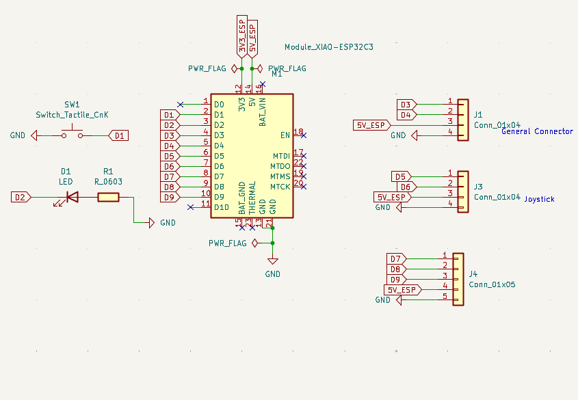
In my design I had the following components:
- Xiao ESP32-C3
- 1 X Resistor
- 1 X LED
- 2 x 4pin connectors
- 1 x 5pin connector
- Push button
I started with opening Kicad and creating a new project and then going to the schematic. I then placed all the components I needed by going to place>place symbols or you could just press A.
I choose generic connectors as the footprint could later be assigned to choose a specific type of connector I wanted same with the other components beside the xiao and push button which I got from the fab library.

I then added global labels to the xiao pins so I can just re-use them with other components instead of having to teadiously wire them. I also added no-connect flags to any pins I didn't need. Both of these can be found in the right toolbar.
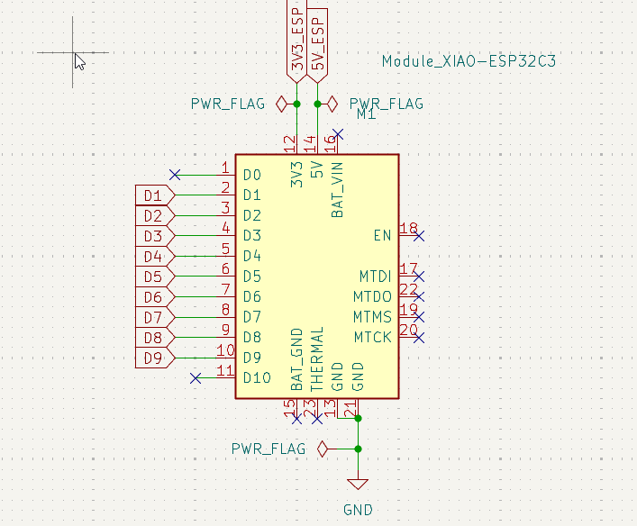
This is what it looked like when I added the the global labels to all the components.
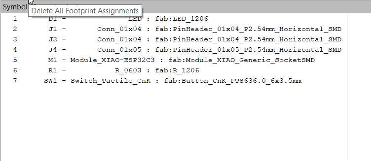
After that I added the footprints to all the components by going to assign footprints.
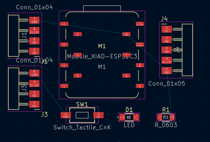
After that I went to the PCB editor and imported the schematic by going to tools>update PCB from schematic.
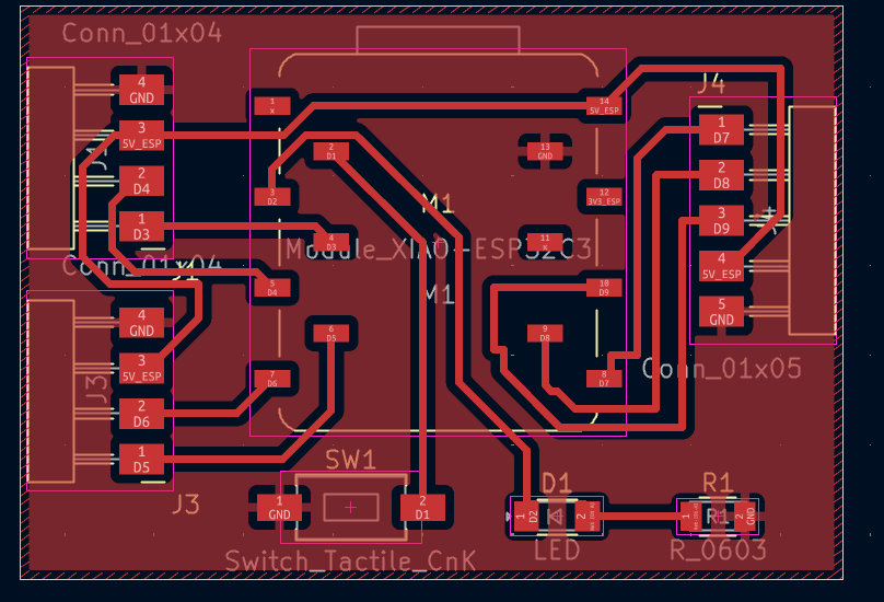
This is what it looked like when I had alligned all the components to my liking.
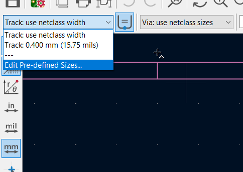
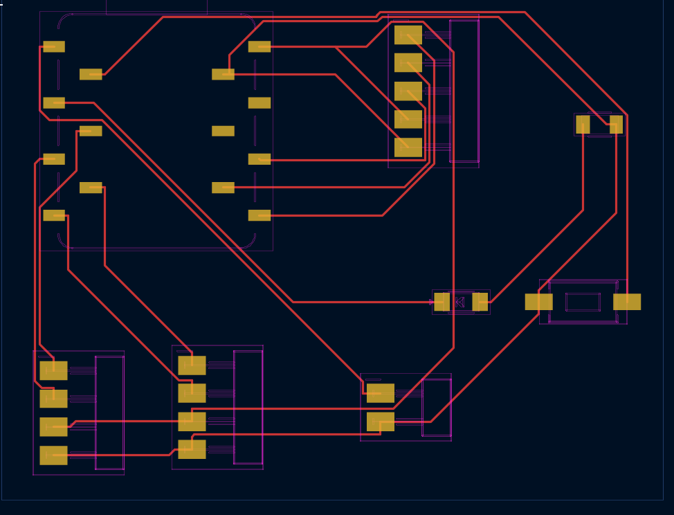
There I went to track and added my size the size of the routes I wanted which was 0.4mm
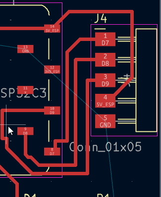
After that I started routing all the components.
Once all the routing was done I first made a rectangle encompassing everything and then added the ground layer by going to draw filled zones and selecting GND.
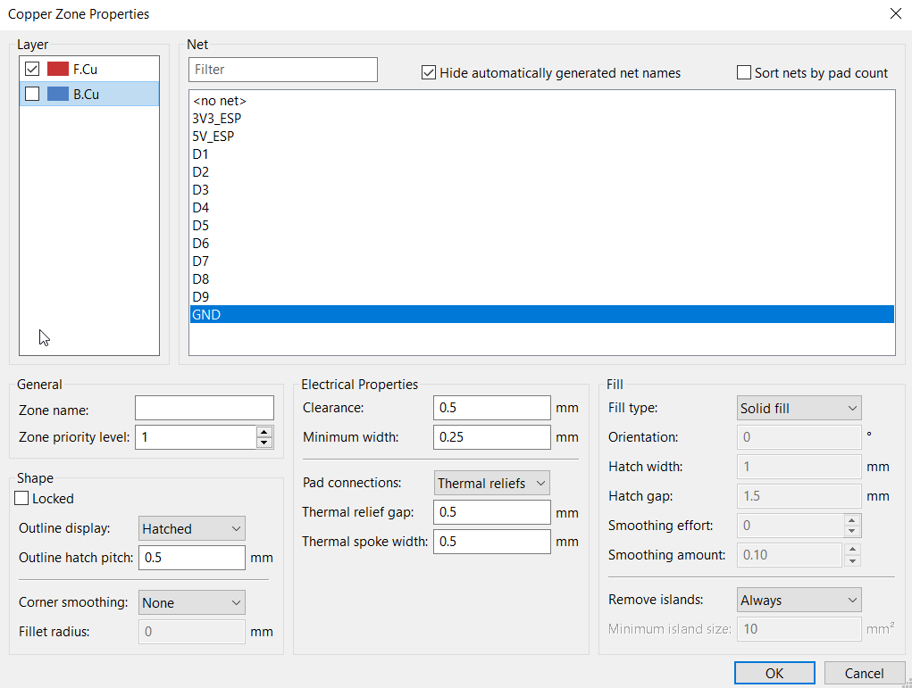
Once I had the area mapped where I wanted the ground layer I pressed B and it filled everything and this is what the end result looks like.
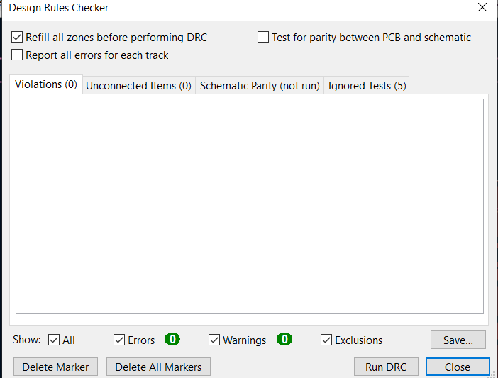
After that I went to design rules and checked the design rules and it showed me that everything was fine.
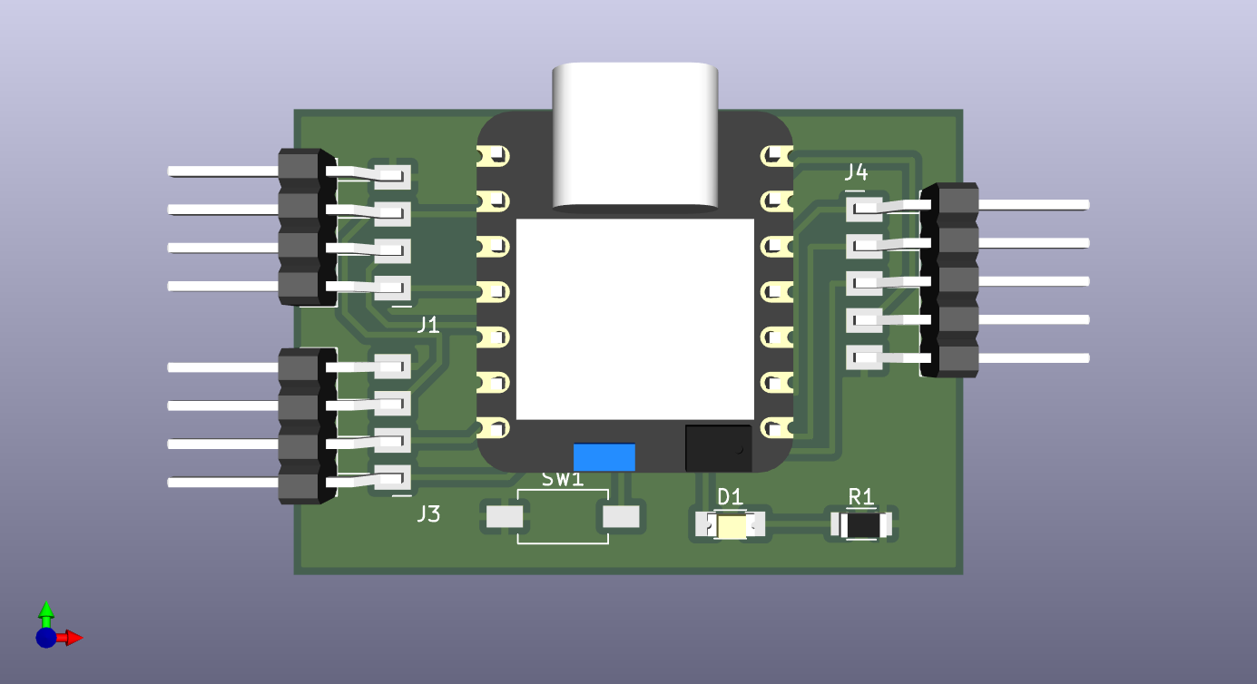
This is what it looked like when I went to the 3d Viewer which gave an accurate image of what it was supposed to look like in reality.
After that I exported the gerber files by going to file>plot and selecting the layers I wanted to export.
FreeRouting
I found out that there are free softwares available online that can route the components for you automtically and freerouting was a popular one. I donwloaded it and then opened it.
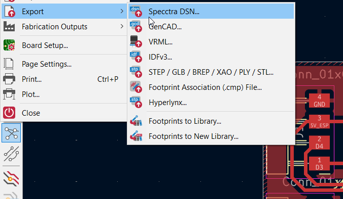
For this you have to export the kicad file in spectraDSN format.
Once that is done I opened the file in freerouting.
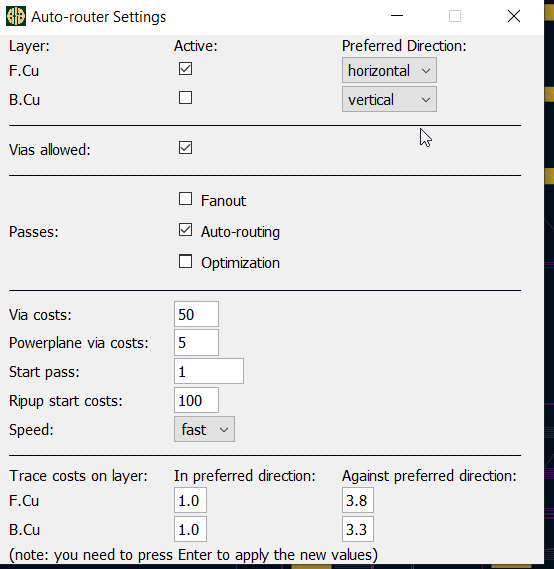
There you can edit the settings as to how the routes you want done.
After that you can press the auto route button and it will automatically do all the routes.
Then you can just save the file and open it in kicad.
Download File
 ← Back to Main Page